by David Armstrong
The amount of water used by the producers of semiconductor devices can be surprising to those of us who don’t work in the industry. Semiconductor chips that we use everyday in our computers, cell phones and automobiles are the result of a manufacturing process that requires ultra-pure water (UPW) at nearly every step. The chips themselves are built upon a silicon wafer that must be cleaned thoroughly before it’s appropriate for use as the foundation for the chips to be built upon its surface. A single 8" wafer, which is the foundation for approximately 100 chips, may require up to 2,000 gallons of UPW to bring it to the necessary level of cleanliness. Figures recently released from the Semiconductor Equipment and Materials International (SEMI) show that approximately 173 million 8" wafers (or their equivalent in other sizes) were projected to be manufactured in 2007. This means that semiconductor wafer producers around the world use more than 450 times the amount of water consumed by the city of Sonoma, CA (population 9,128). Some chip manufacturers consume as much as 1 billion gallons per year per location.
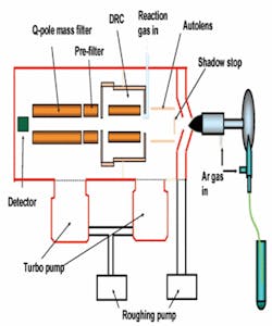
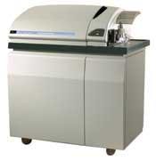
Figure 1. A diagram the PerkinElmer Sciex™ ELAN DRC II ICP-MS system with the Dynamic Reaction Cell
Such high usage of UPW places stresses on the costs of semiconductor producers and the environment. By some estimates, every dollar’s worth of water purchased by a semiconductor producer requires $20 more to bring it to UPW levels and another $10 to treat it for discharge. Additionally, semiconductor production is moving into geographic areas with limited water supplies. Excessive water use can create hardships for households, local farmers and even wildlife if water levels in local streams and aquifers are brought to dangerously low levels. In response, semiconductor producers are focusing on ways to recycle, reuse and, in general, reduce the amount of UPW used in their processes. From the initial acquisition to the eventual discharge, analytical testing of its purity is of paramount importance if decision makers are to be properly informed of the true content of the water used in a semiconductor facility.
One of the important tests performed on UPW is the analysis of low level metals. A widely used analytical tool for such measurement is the Inductively Coupled Plasma-Mass Spectrometer (ICP-MS). This tool, as it’s called in the semiconductor industry, provides part per trillion (ppt) analysis of nearly every metal of interest in under five minutes. Today, the semiconductor industry has technologies that can provide rapid and accurate analyses of UPW.
The operation of an ICP-MS system can be easily explained. The right side of Figure 1 shows the UPW sample (contained in the test tube), which is aspirated by a nebulizer that shatters it into droplets of about 1 micron (µm) in diameter. These droplets are then passed through an argon plasma that quickly dries the droplet, dissociates the metals from any species to which they may be chemically bound, and removes one electron from each atom to form a singly charged ion. This singly charged ion is projected through a focusing system (autolens), through a mass spectrometer (Q-pole mass filter), and finally is measured by a detector which actually counts the number of ions that impact its active surface. The number of ions counted is correlated to concentration. This type of technology is relatively straight forward, yet there can still be challenges.
For example, most elements have several isotopes that can be used by the ICP-MS in its measurement. It’s most desirable to use the isotope of highest abundance since that gives the greatest number of ions to count for any given concentration of the element measured. If we examine the isotopes of calcium, we find– of the six naturally occurring isotopes – 96.9% of them are at mass 40 (40Ca). An argon plasma is used to generate the singly charged ions measured by the ICP-MS. As nature would have it, 99.6% of the argon atoms are found at mass 40 (40Ar) also. In traditional ICP-MS systems, this results in a signal at mass 40 that’s swamped by a deluge of counts from 40Ar. In such a situation, the only choice is to select an alternate isotope such as 44Ca that greatly reduces detection limits achievable. Fortunately, technology exists that can most effectively removed the 40Ar signal while preserving the 40Ca resulting in extremely low detection limits for this important element.
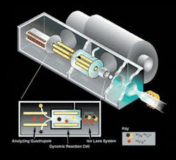
A dynamic reaction cell (DRC) provides impressive improvements in instrument performance while requiring almost no additional operator attention. A DRC contains a quadrupole mass spectrometer housed inside a pressurized cell. As seen in Figure 1, the reaction cell is physically placed between the instrument’s ion focusing system and the filtering quadrupole. In the reaction cell, the ions of 40Ar react very quickly (exothermally) with a reaction gas that has been introduced, while the 40Ca ions react very slowly (endothermally) with the gas. As a result of these reactions, the element of interest (calcium) can be measured without interference from the argon coming from the plasma.
In a second example, the reaction cell can also provide freedom from polyatomic species. Once again, iron has several isotopes but the isotope of greatest abundance (91.8%) is at mass 56 (56Fe). The argon from the plasma unfortunately combines with oxygen from the water to form the polyatomic species ArO. Looking at the natural abundances of argon and oxygen we find that nearly all of the ArO formed will be right at mass 56 (40Ar16O). Fortunately, this polyatomic species is removed by the reaction cell in the same manner as is the argon. The removal of the 40Ar16O interferent from the 56Fe signal is shown in Figure 2.
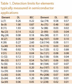
In a similar manner to that just described, the reaction cell removes those interferences that potentially can limit the very low detection limits achievable with ICP-MS instrumentation. Figure 3 shows Detection Limits (DL) achievable with the ELAN DRC II system. Elements shown in red are measured using the reaction cell while those shown in blue were measured without use of the reaction cell. Switching from reaction cell mode to standard mode is performed automatically by the instruments software.
Background Equivalent
Concentrations are shown to demonstrate that the background in all cases has been reduced to single ppt levels or lower. All detection limits are three sigma and are determined using a 1-second integration. A typical analysis of UPW for up to 32 elements can be competed in approximately five minutes.
Conclusion
Demand for high purity water in the semiconductor industry is extremely high and that demand can be expected to rise as the semiconductor industry continues to grow. As new sources of water are explored and the need for low detection limits increases, ICP-MS instrumentation will provide ppt level detection limits quickly and readily. Dynamic reaction cell technology provided with the PerkinElmer Sciex™ ELAN DRC II system has been demonstrated to provide this exceptional performance rapidly and with minimal operator intervention.
About the Author: David Armstrong is Chemical & Semiconductor Marketing Leader at PerkinElmer Life and Analytical Sciences, which is based in Shelton, CT. Contact: 800-762-4000 or http://las.perkinelmer.com
